TTL COMPUTER BY ALESSIO LOMBARDO
[HOME] [WORKLOG]
[HARDWARE]
[CONTACT-ME]
[
![]() ]
]
"ALU" Section
Architecture
The ALU section,
as the section Registers,
is used both Lite and Full version. It consists of two parts: The proper ALU ("ALU Core" Card) and
the register "C" ("ALU Register" Card).
The ALU is the calculation unit. Here, logical and arithmetic operations occur
between a register A and a register B. The ALU is composed of 4 DM74181N IC of
National Semiconductor. Each IC execute 4-bit computations and therefore 4 IC in
parallel are needed for execute 16-bit calculations. These IC also have two "Flags":
The Carry Out (used as Overflow in the last IC) and the equality signal (this is
active if A=B). The Overflow signal is needed only when making arithmetic
operation and not logic operation. So with using a SN74LS02N IC the Overflow
signal will be disabled if you are making a logic operation (M Pin is High).
Also with using a SN74ALS21N IC is possible connect together the 4 signals "A=B"
and permit the activation of a single signal when the two 16-bit Data are equal.
During the preliminary tests, I realized that the 74181 were hot. So, also as
embellishment, I decided to add a fan above the 4 IC.
The Register C is structurally similar to the registers A and B already thoroughly analyzed in the "Registers" Page. This register is a "barrier" between the ALU and the Data Bus that is, avoid that the input data end up in the out pin of the ALU. Also, the result of an operation it can not be directly written to a register A or B because they are already involved to make the itself operation. So it need a registry that keep the result and then, if necessary, transfer it on the desired register.
The ALU and the Register C are controlled by a single 9-bit Control Bus. Is presented below a table of operations that the ALU and the Registers C can do.
| Code | Operation | |||||
| ALU | ALU FAN | REGISTRER C | ||||
| FUNCTION | MNEMONIC CODE | |||||
| 000000 | X | XX | A plus 1 | INC | Unknow | Unknow |
| 000001 | X | XX | A | NULA | Unknow | Unknow |
| 000011 | X | XX | A+B | OR | Unknow | Unknow |
| 000110 | X | XX | 0 | CLR | Unknow | Unknow |
| 001100 | X | XX | A minus B | SUB | Unknow | Unknow |
| 001101 | X | XX | A minus B minus 1 | CMP | Unknow | Unknow |
| 010010 | X | XX | A plus B plus 1 | ADC | Unknow | Unknow |
| 010011 | X | XX | A plus B | ADD | Unknow | Unknow |
| 010110 | X | XX | AB | AND | Unknow | Unknow |
| 011001 | X | XX | A plus A | SHFT | Unknow | Unknow |
| 011110 | X | XX | A | NULA | Unknow | Unknow |
| 011111 | X | XX | A minus 1 | DEC | Unknow | Unknow |
| 10000X | X | XX | A | NOTA | Unknow | Unknow |
| 10001X | X | XX | A+B | NOR | Unknow | Unknow |
| 10011X | X | XX | 0 | CLR | Unknow | Unknow |
| 10100X | X | XX | AB | NAND | Unknow | Unknow |
| 10101X | X | XX | B | NOTB | Unknow | Unknow |
| 10110X | X | XX | A(+)B | XOR | Unknow | Unknow |
| 11001X | X | XX | A(+)B | XNOR | Unknow | Unknow |
| 11010X | X | XX | B | NULB | Unknow | Unknow |
| 11011X | X | XX | AB | AND | Unknow | Unknow |
| 11100X | X | XX | 1 | PSET | Unknow | Unknow |
| 11110X | X | XX | A+B | OR | Unknow | Unknow |
| 11111X | X | XX | A | NULA | Unknow | Unknow |
| XXXXXX | 0 | XX | Unknow | Unknow | Off | Unknow |
| XXXXXX | 1 | XX | Unknow | Unknow | On | Unknow |
| XXXXXX | X | 00 | Unknow | Unknow | Unknow | Read |
| XXXXXX | X | 01 | Unknow | Unknow | Unknow | Sleep |
| XXXXXX | X | 10 | Unknow | Unknow | Unknow | Trasparent |
| XXXXXX | X | 11 | Unknow | Unknow | Unknow | Write |
"plus" = Arithmetic addition / "+" = Logic OR / "(+)" = Logic XOR / "minus" = Arithmetic subtraction / Red Code = 1's complement
Cards
The "Registers" section is composed of 3 cards grafted together with connectors. The 3 cards are:
ALU - Core: It contains the 4 74181 IC, the management of "Overflow" and "A=B" signals and a LED Visualizer
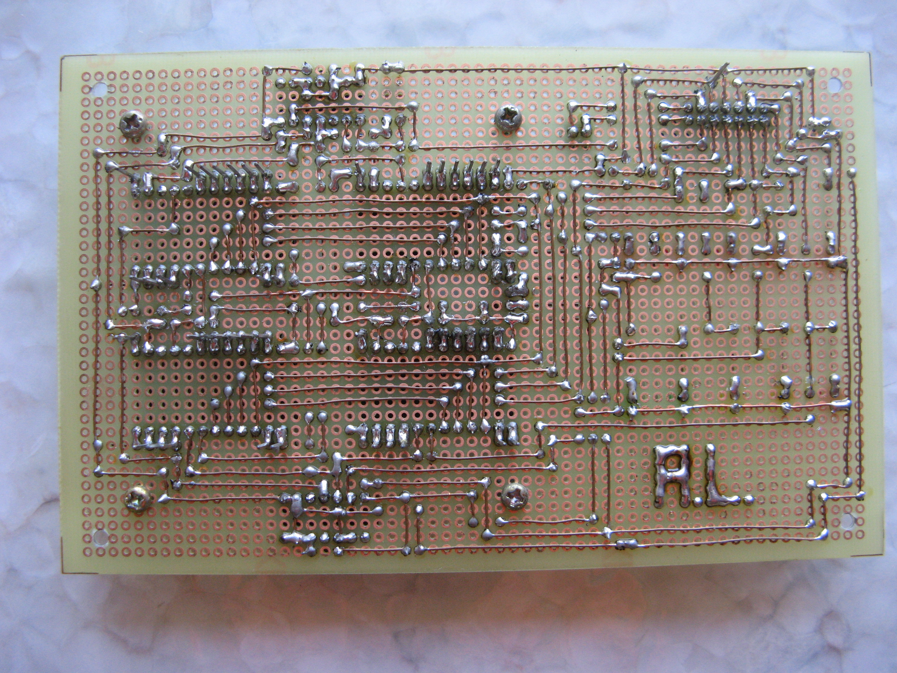
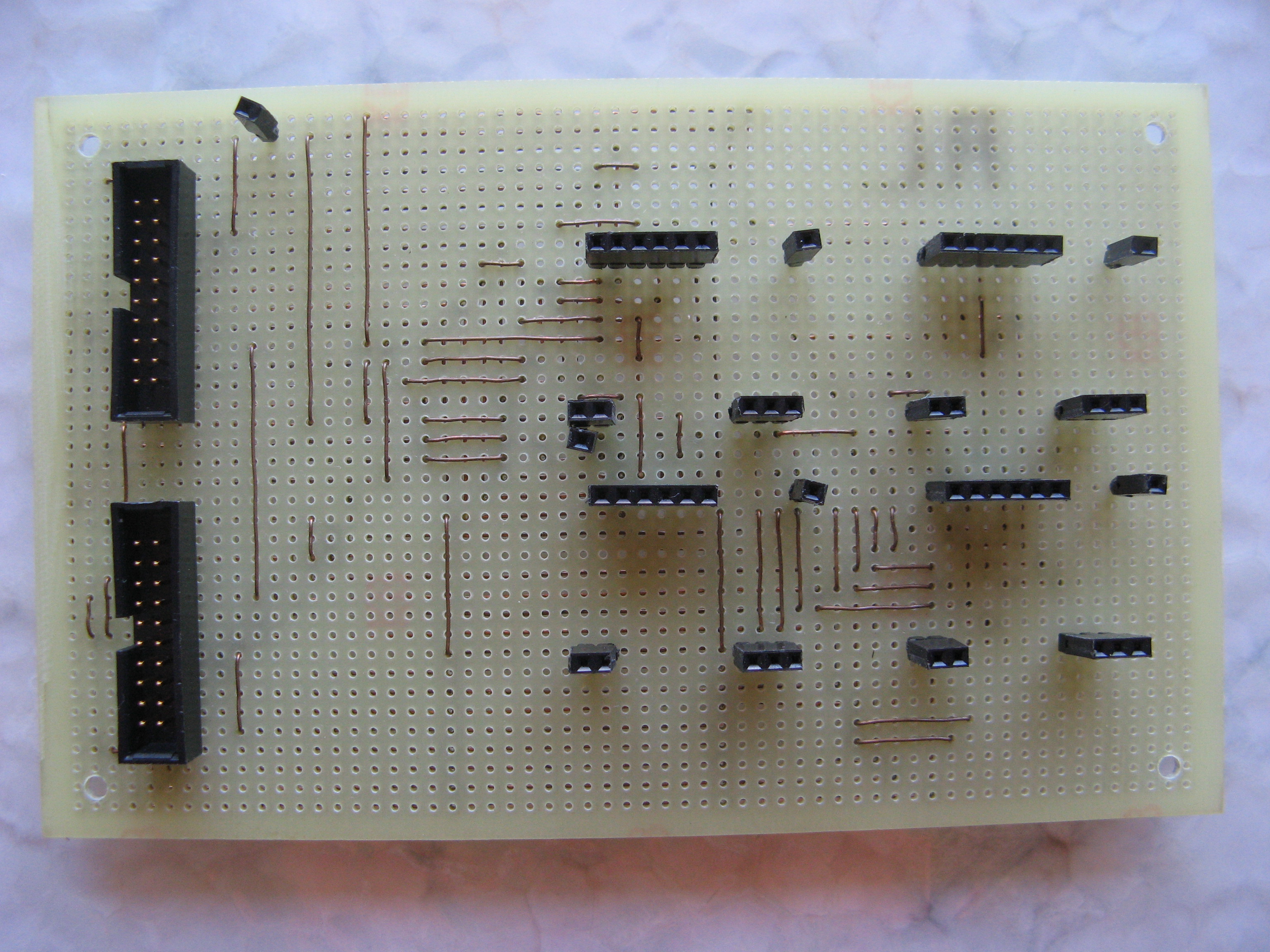
ALU - Internal Bus: It distributes the input data from "Registers" section to the "ALU Core" Card
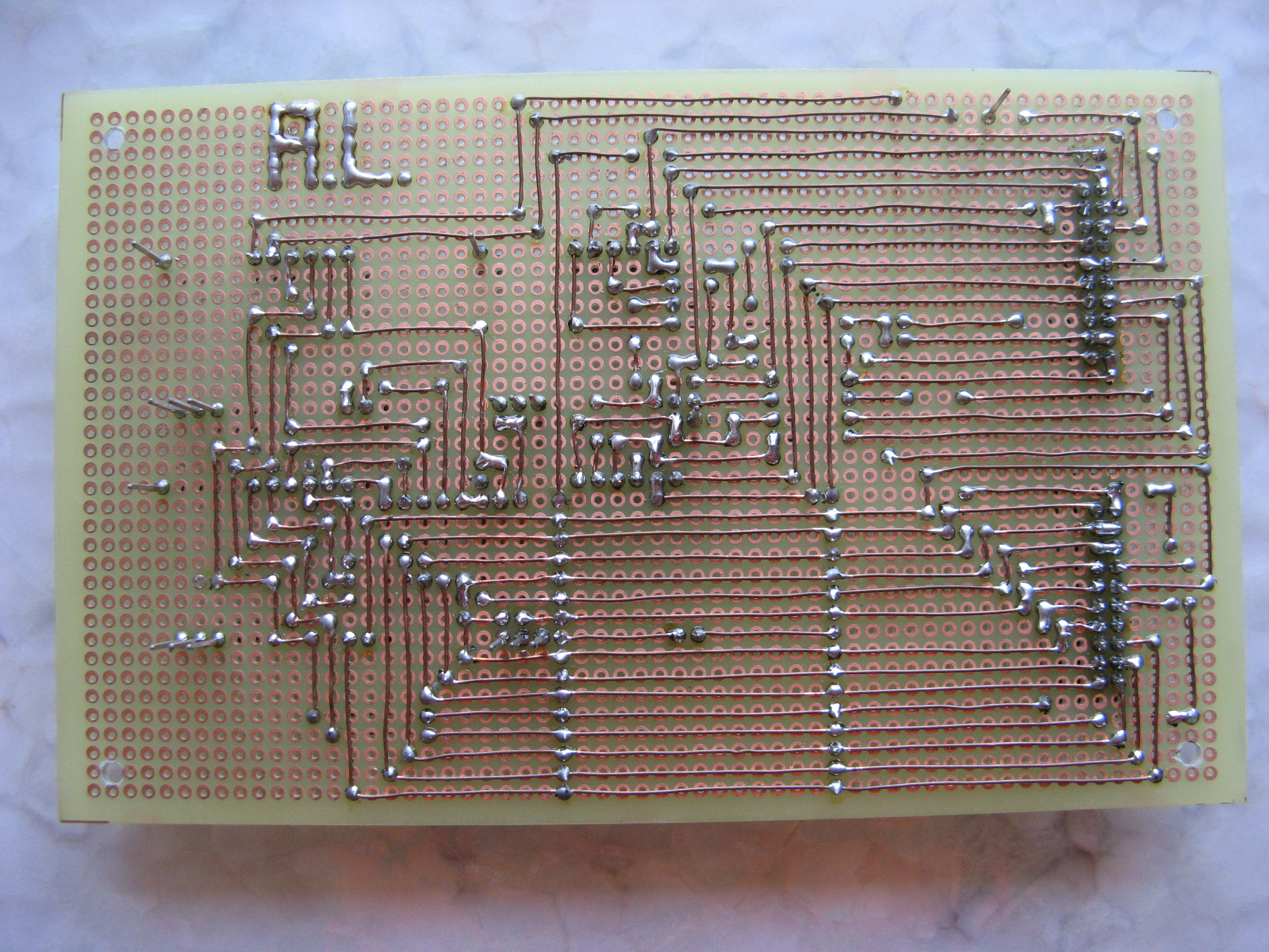
ALU - Register: It contains the register "C" and the Data Bus
Circuit Diagrams
Under design...
Photogallery
This is the photogallery of the "ALU" section. Click on photos to enlarge.
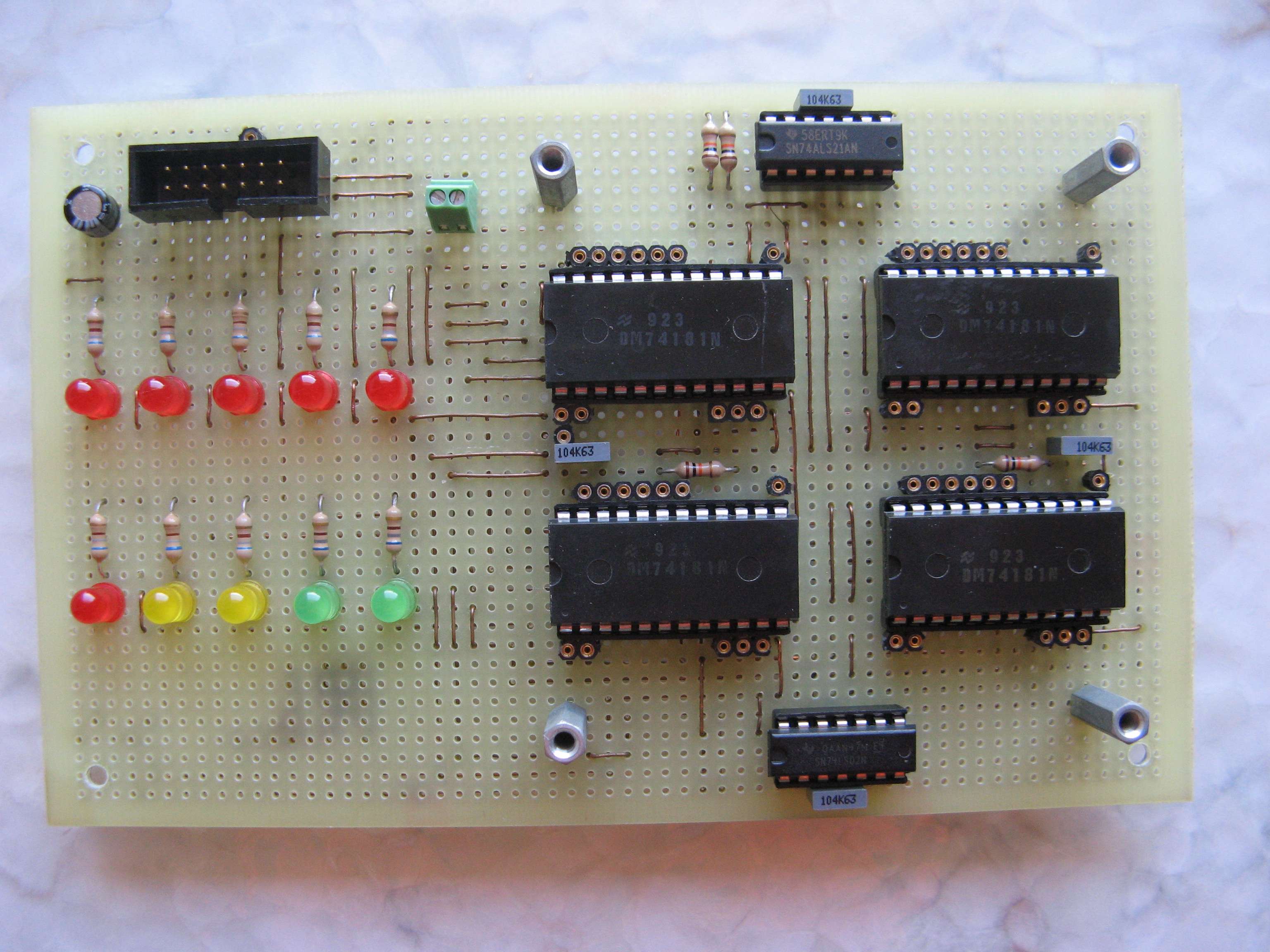
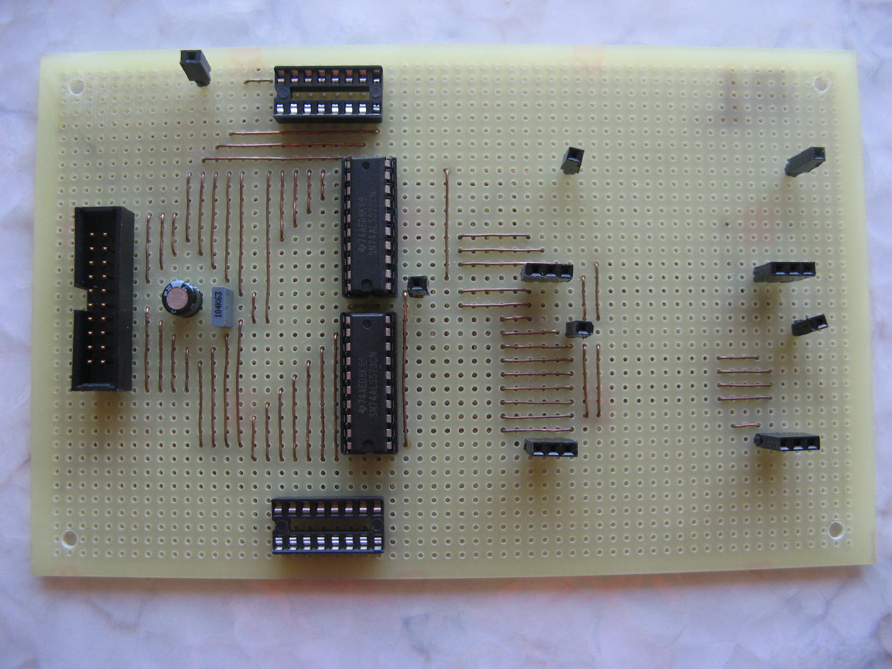
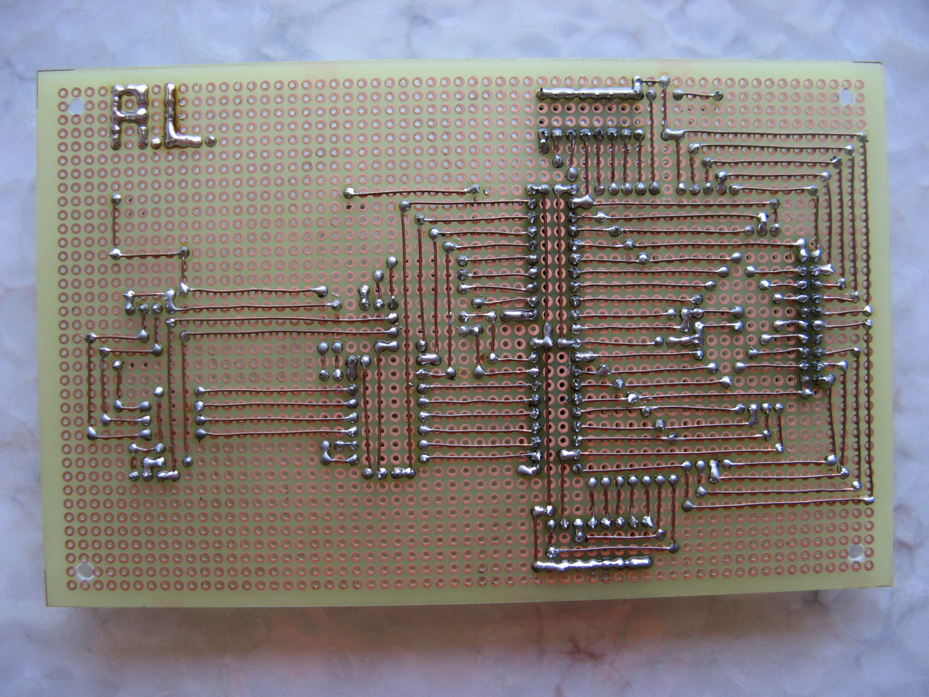
From top to bottom: "ALU - Core" Card, "ALU - Internal Bus" Card, "ALU - Register" Card